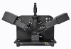
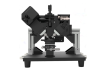
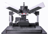
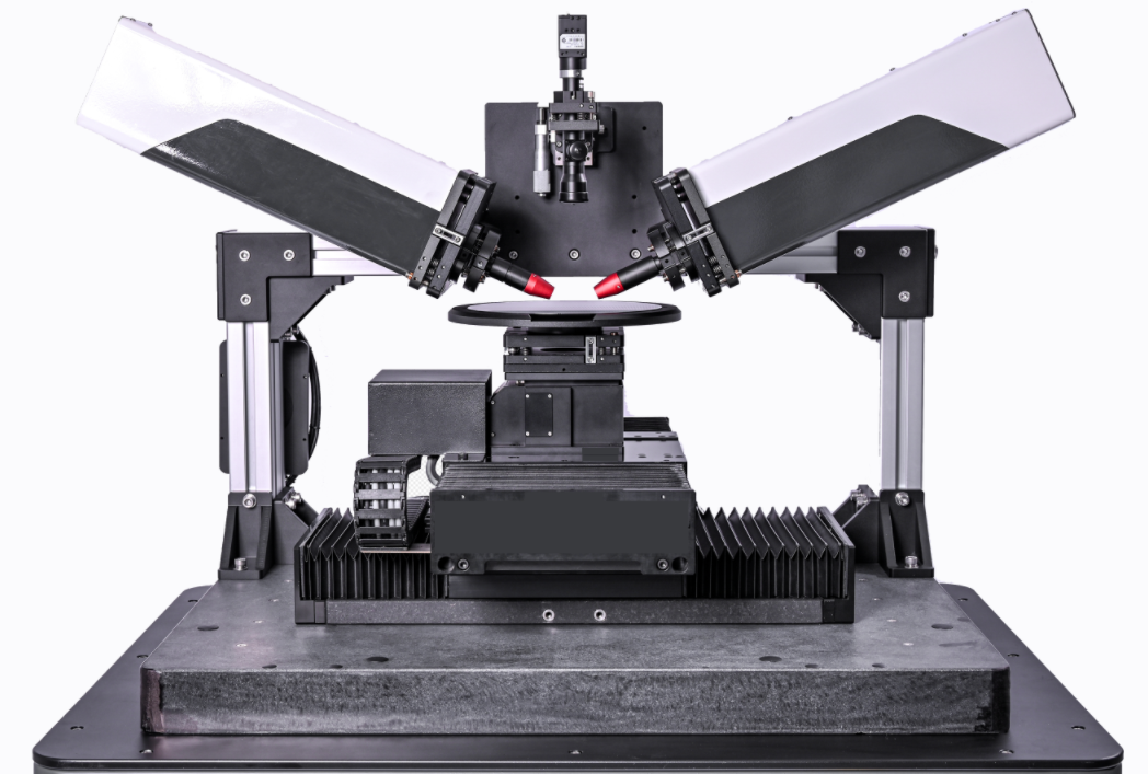
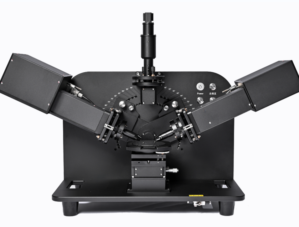
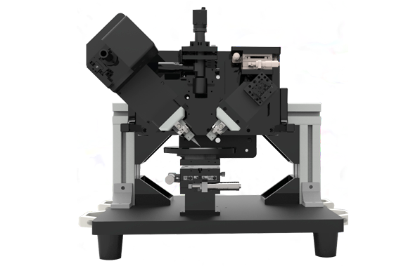
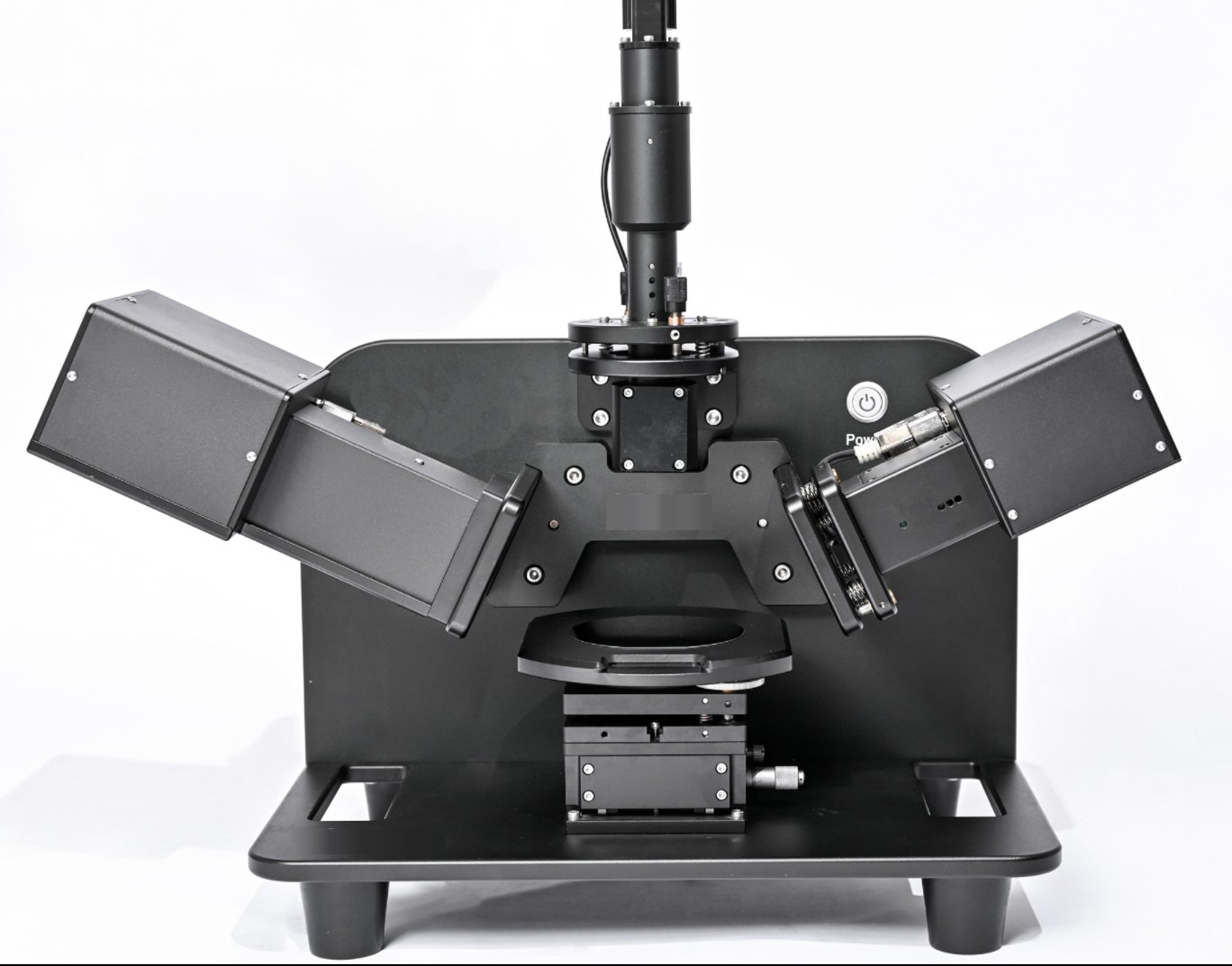
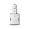
Ellipse Measurement System

Tổng quan về sản phẩm
Dựa trên sự điều chế của bộ bù xoay kép, phép đo nhanh 16 phần tử của toàn bộ ma trận Muller được thực hiện Được sử dụng để mô tả độ dày màng mỏng đẳng hướng/dị hướng, hằng số quang học và cấu trúc nano
Công nghệ cốt lõi
- Công nghệ điều khiển đồng bộ bộ bù xoay kép
- Công nghệ bộ bù không sắc phổ rộng,
- Công nghệ phát hiện ít đốm Thuật toán hiệu chuẩn độ chính xác của thiết bị
- Công nghệ thay đổi góc và tiêu điểm hoàn toàn tự động, đo nhanh bằng một phím
- Bề mặt quả tương tác giữa người và máy Wizard, trải nghiệm vận hành phần mềm thuận tiện
- Cơ sở dữ liệu vật liệu phong phú và thư viện mô hình thuật toán, khả năng phân tích dữ liệu mạnh mẽ


Technical Characteristics


Mapping
Spectral Ellipsometry Solution
It meets the needs of multi-point custom mapping of large-size substrates, supports size customization, real-time offline detection and output of film thickness morphology distribution and data reports, and is widely used in equipment manufacturers/Fab-level coating uniformity rapid measurement and characterization

High-Precision Spectroscopic Ellipsometer
It can realize scientific research/enterprise-level high-precision and rapid spectral ellipsometry measurement, support multi-angle, low-spot and other high-compatibility flexible configuration, multi-function module customized design, and is widely used in optical communication/OLED/TP/transparent conductive film and other applications involving transparent substrate coating measurement and characterization
Spectral Ellipsometry Solution for Micro
With the image recognition system, it can meet the needs of high-precision and fast spectral ellipsometry measurement of various micro-regions of various objects to be measured at the scientific research/enterprise level
Economical Spectral Ellipsomemeter solution
It can meet the cost-effective measurement needs of most of the spectral ellipses of scientific research/enterprise films, quickly characterize the thickness and optical constants of thin films, and can achieve one-click measurement for conventional single-throw Si/InP/GaAs and other substrate coatings
Mapping
Spectral Ellipsometry Solution
It meets the needs of multi-point custom mapping of large-size substrates, supports size customization, real-time offline detection and output of film thickness morphology distribution and data reports, and is widely used in equipment manufacturers/Fab-level coating uniformity rapid measurement and characterization

Technical Specifications:

Các Sản Phẩm Liên Quan


- Home Home
- About Us About Us
- All Products All Products
- Fabs Fabs
- Labs Labs
- Courses Courses
- Services Services
- Application Application
- Accessories Accessories
- News & Events News & Events
- Contact Us Contact Us
- Request Quotation Request Quotation
- Vibration Isolator Vibration Isolator
- UV ozone UV ozone
- Insitu AFM SEM Insitu AFM SEM
- ALD ALD
- TEM Consumables TEM Consumables