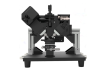
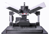
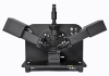
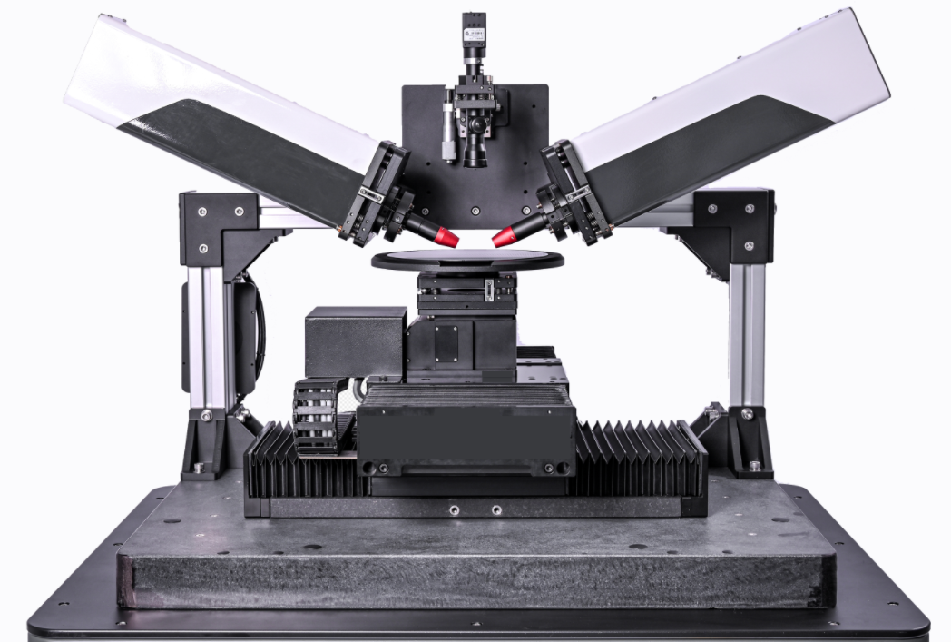
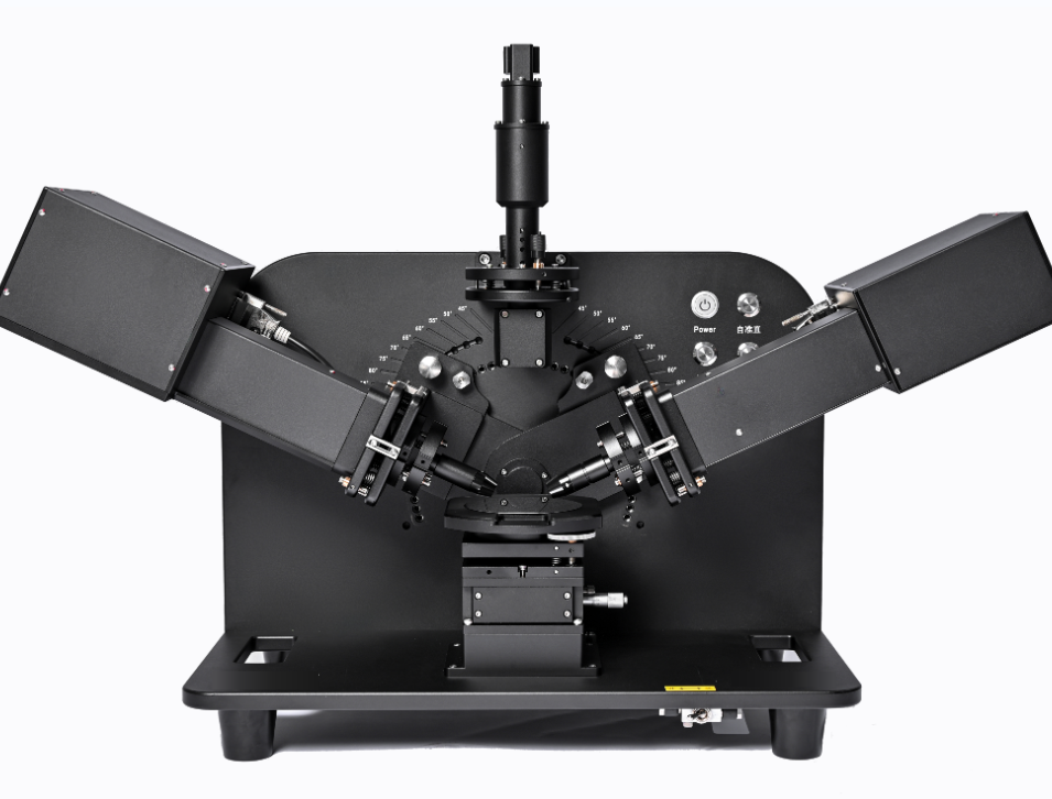
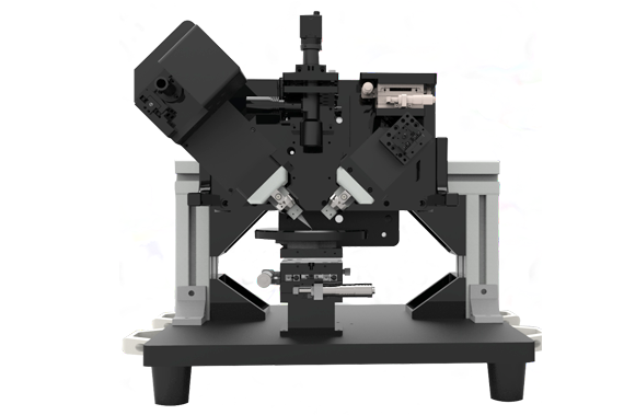
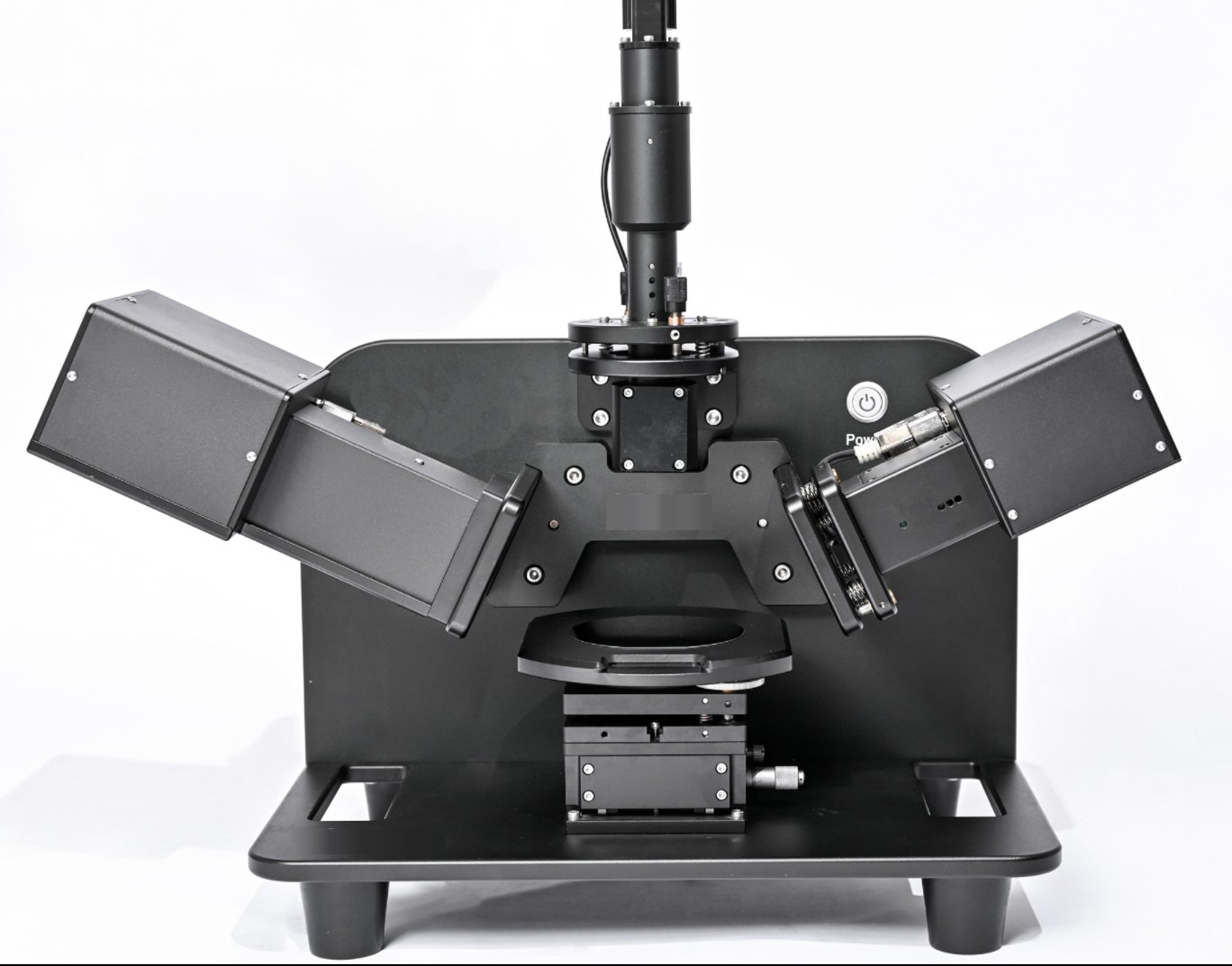
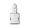


Berdasarkan modulasi pemampas putaran berganda, pengukuran pantas 16 elemen keseluruhan matriks Muller direalisasikan
Ia digunakan untuk pencirian ketebalan filem nipis isotropik/anisotropik, pemalar optik, dan struktur nano.
It meets the needs of multi-point custom mapping of large-size substrates, supports size customization, real-time offline detection and output of film thickness morphology distribution and data reports, and is widely used in equipment manufacturers/Fab-level coating uniformity rapid measurement and characterization

It can realize scientific research/enterprise-level high-precision and rapid spectral ellipsometry measurement, support multi-angle, low-spot and other high-compatibility flexible configuration, multi-function module customized design, and is widely used in optical communication/OLED/TP/transparent conductive film and other applications involving transparent substrate coating measurement and characterization

With the image recognition system, it can meet the needs of high-precision and fast spectral ellipsometry measurement of various micro-regions of various objects to be measured at the scientific research/enterprise level

It can meet the cost-effective measurement needs of most of the spectral ellipses of scientific research/enterprise films, quickly characterize the thickness and optical constants of thin films, and can achieve one-click measurement for conventional single-throw Si/InP/GaAs and other substrate coatings

It meets the needs of multi-point custom mapping of large-size substrates, supports size customization, real-time offline detection and output of film thickness morphology distribution and data reports, and is widely used in equipment manufacturers/Fab-level coating uniformity rapid measurement and characterization
