Novel Hyperspectral Microsystem: Imaging & Analysis in One
Introduction
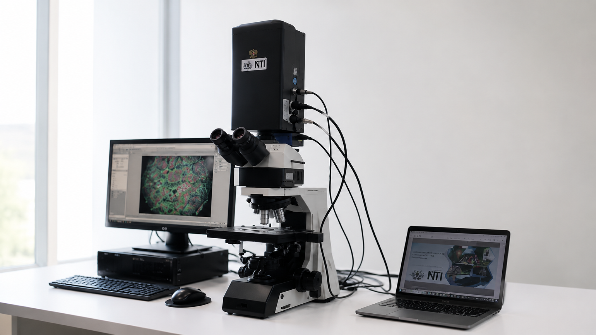
Microscopic imaging is an indispensable tool in research fields such as cell biology, materials science, pharmaceutics, hematology, and medical immunology. Conventional microscopy systems, however, often separate image acquisition, data processing, and quantitative analysis into distinct stages, requiring researchers to rely on multiple software tools and workflows to complete a full study. To address this fragmentation, Hong Kong NTI Limited has developed a "Novel Hyperspectral Microsystem" designed to integrate imaging, processing, and analysis into a single, unified system, while meeting research-grade requirements for hyperspectral microscopic imaging.
This article provides a technical overview of the system, covering its hardware architecture, imaging capabilities, software platform, and representative real-world applications.
Technical Architecture and Core Components
1. Optical Resolution and Three-Dimensional Imaging
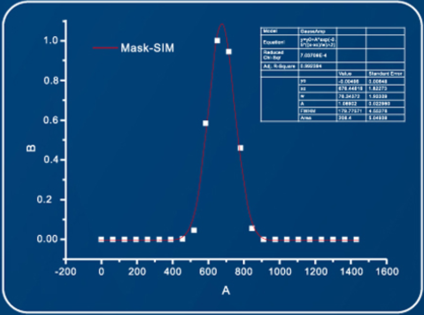
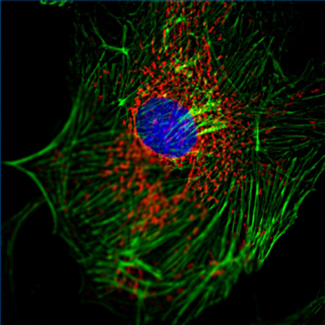
The system achieves an optical resolution of 240 nm in the xy plane and 600 nm along the z-axis, placing it among systems suitable for studying fine microscopic structures. It effectively removes stray light originating outside the focal plane, and employs multi-layer stacking to construct high-definition three-dimensional images.
2. Long-Life, High-Power Independent LED Fluorescence Illumination
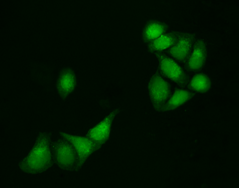
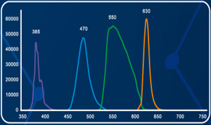
Illumination is provided by a four-wavelength independent LED fluorescence light source characterized by high brightness and a long operational lifespan. The source supports high-speed wavelength switching, which significantly reduces photobleaching of samples. Fiber-optic coupling further ensures uniform illumination across the entire field of view.
3. Research-Grade sCMOS Camera
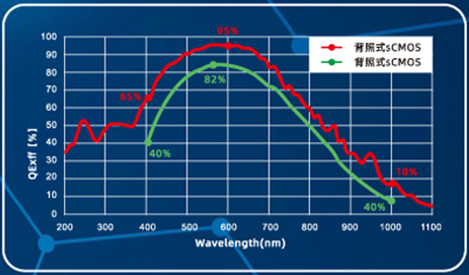
At the core of the imaging pipeline is a back-illuminated, research-grade monochrome sCMOS camera with the following specifications:
- Sensor size: 1.2 inches; pixel size: 6.5 × 6.5 μm
- Quantum efficiency: 95% @ 600 nm
- Frame rate: up to 100 fps @ 2048 × 2048 resolution
These specifications enable the system to capture high-sensitivity, high-resolution images at high speed—an essential capability for studying fast, dynamic biological phenomena in near real time.
4. Research-Grade Software Platform (SRF)
The system is equipped with a dedicated software platform, SRF, which integrates three core functional areas:
- Image Acquisition — Five-dimensional (xyzλt) acquisition covering spatial coordinates (x, y, z), wavelength (λ), and time (t), with fully automated, multi-dimensional workflow control.
- Image Processing — 3D reconstruction and visualization, co-localization processing and linkage, adjustment of brightness/contrast/threshold, image flipping and mirroring, background removal, dynamic image (time-lapse) generation, stack processing, and region-of-interest (ROI) processing.
- Analysis — Quantitative analysis of parameters such as distance, perimeter, area, circularity, and maximum/minimum grayscale values; co-localization analysis; cell counting; particle counting; protein tracking; subpopulation analysis; and cell cycle analysis.
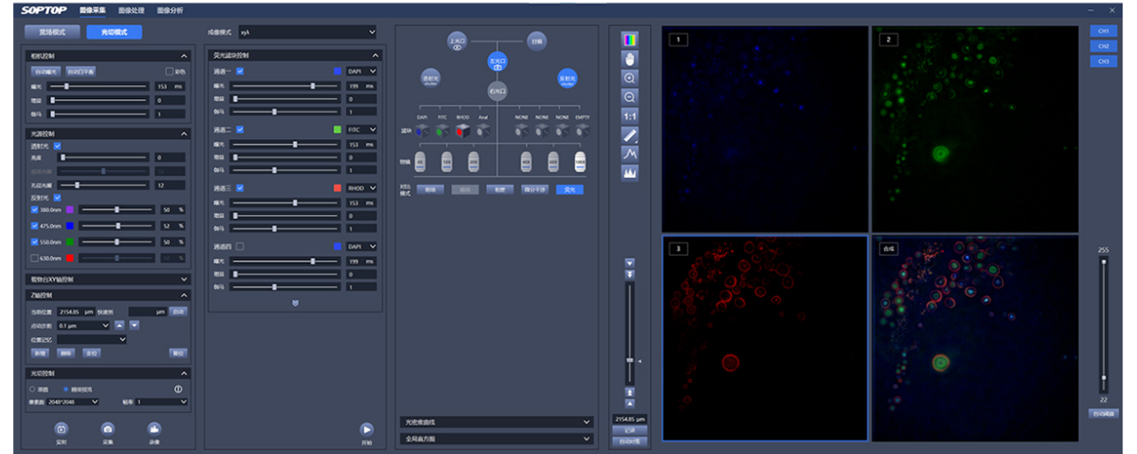
The integration of these three functional layers into a single platform reflects the system's central design philosophy: minimizing workflow complexity from data acquisition through to final analysis.
Case Studies of Practical Application
According to the product documentation, the system has been applied across a diverse range of case studies, illustrating the versatility of hyperspectral microscopic imaging across multiple disciplines:
- Interactions between nanomaterials and microbial cells, using titanium dioxide (TiO₂) nanoparticles as a case example.
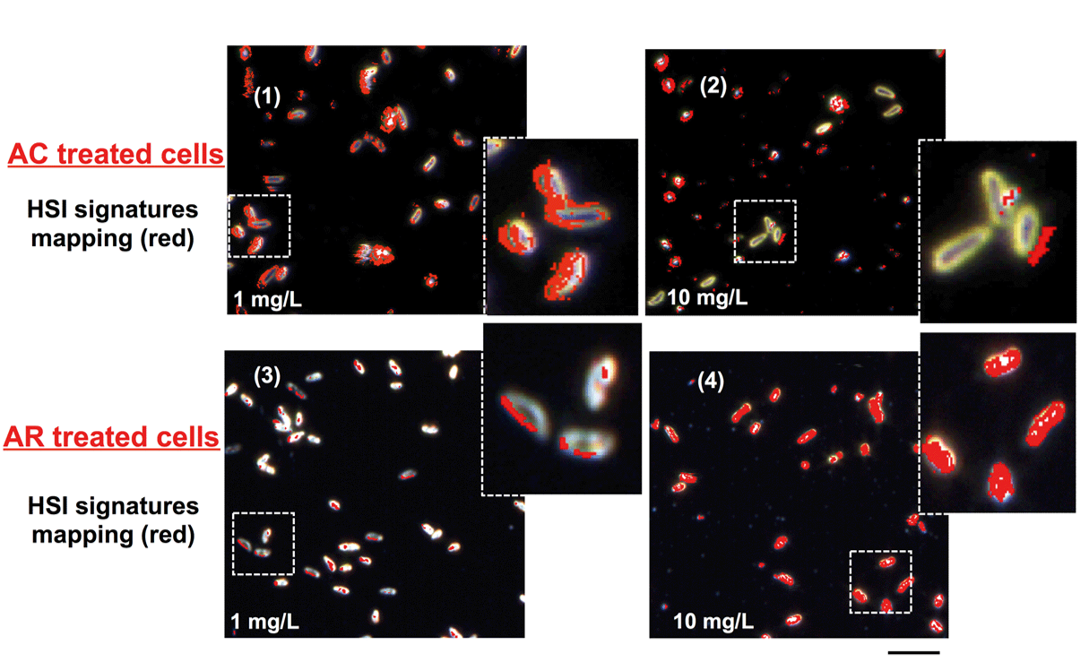
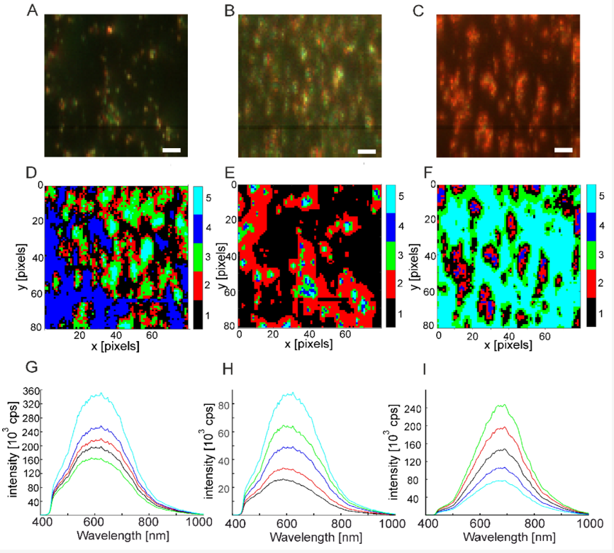
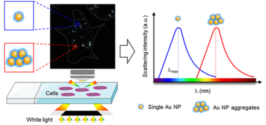
- Detection of nanoparticles in cell cultures, using gold (Au) nanoparticles.
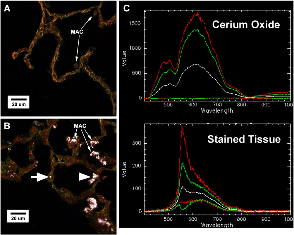
- Detection of iron oxide nanoparticles in cell cultures, alongside visual and spectral identification of cerium dioxide (CeO₂) nanoparticles in tissue.
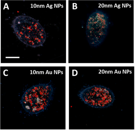
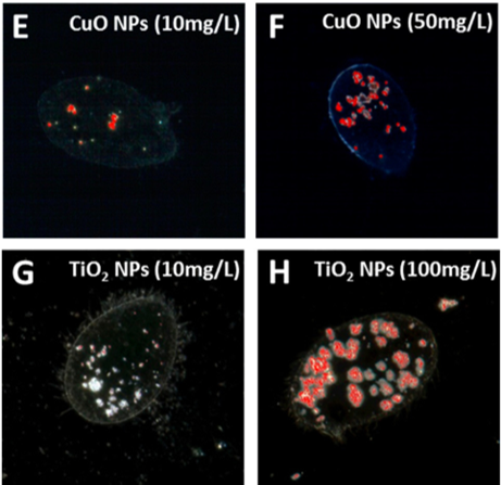
- In vivo imaging and characterization of various metal nanomaterials within multicellular organisms.
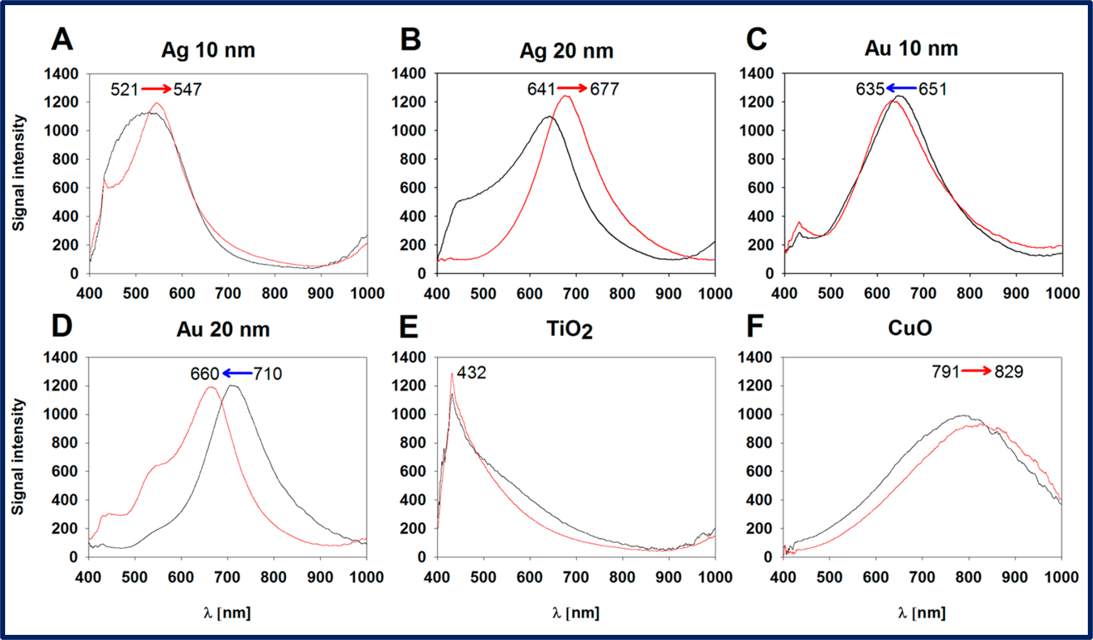
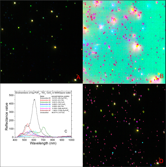
- Imaging and identification of various metal nanomaterials in environmental samples.
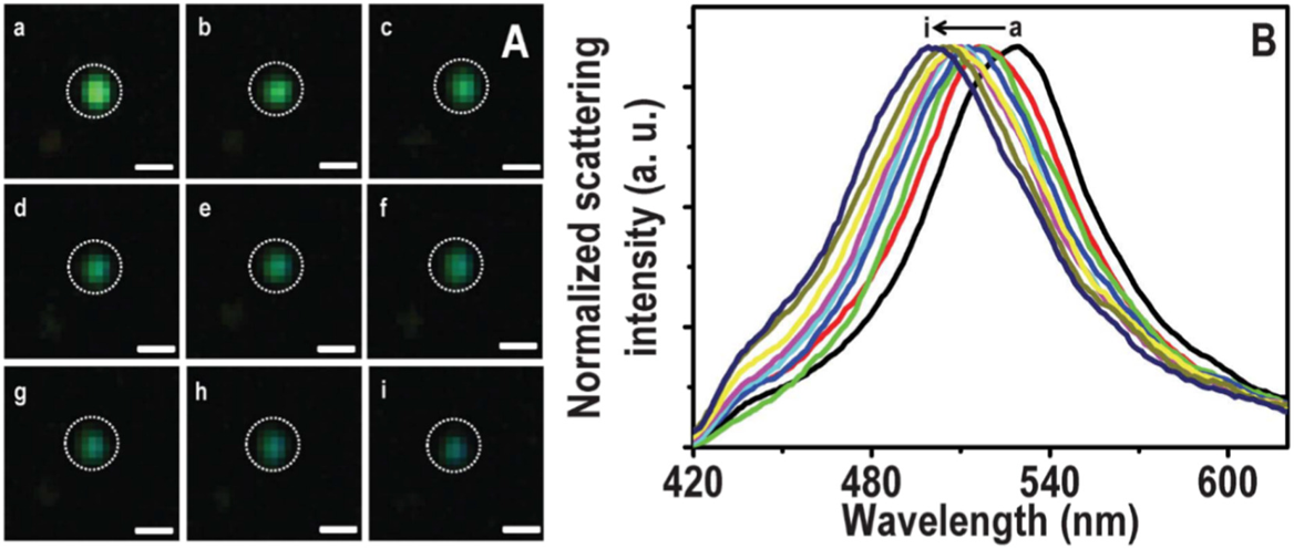
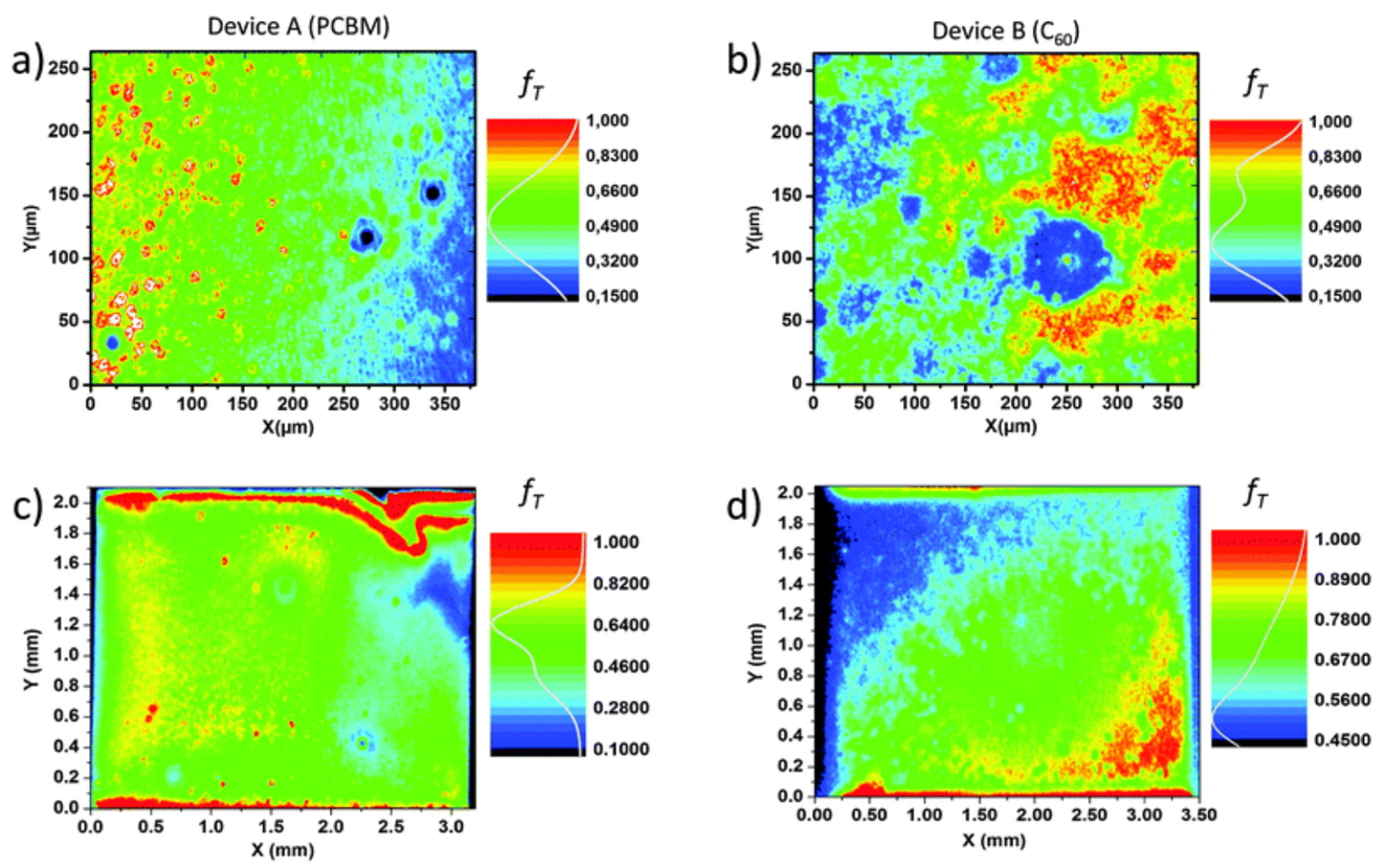
- Spatial and spectral analysis of perovskite nanomaterials.
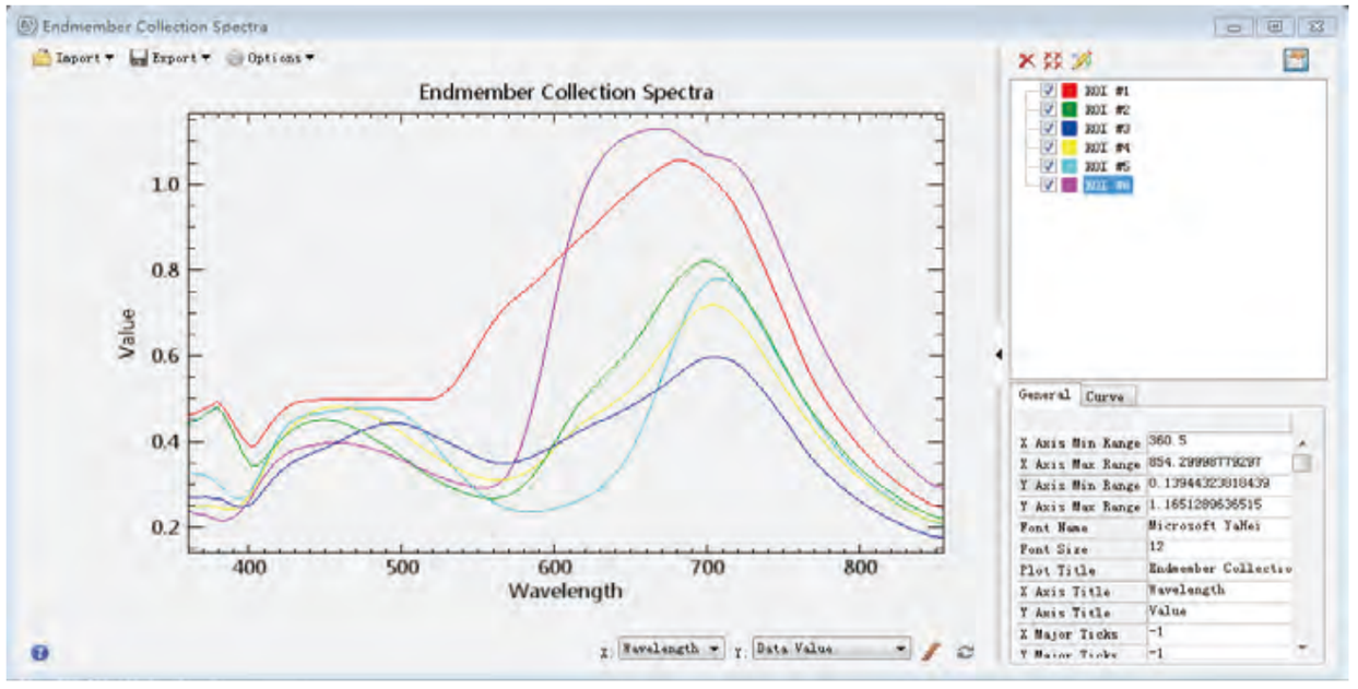
- Characteristic spectral analysis of fabric (textile) fibers under a 50× objective lens.
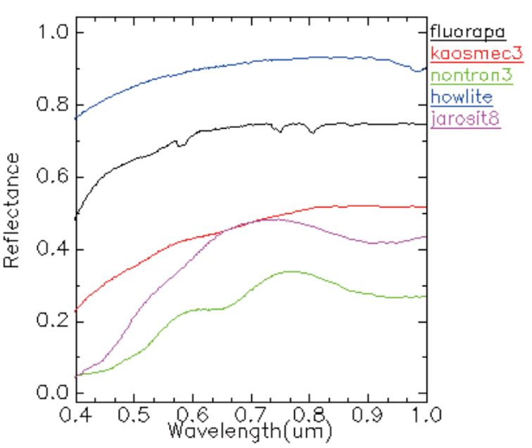
- Mineral composition analysis, including spectral reflectance curves of minerals such as datolite and calcium borosilicate.

These examples demonstrate that the system is applicable not only in biology and nanotechnology research, but also in materials science, environmental science, and geology—leveraging its core strength of image–spectral integration across the visible-to-near-infrared range (400–1000 nm).
Conclusion
The Novel Hyperspectral Microsystem presented in this article is a visible-to-near-infrared (400–1000 nm) hyperspectral microscopic imaging system built around three defining features: (1) image–spectral integration in support of a smart digital future, (2) nanoscale-resolution three-dimensional imaging, and (3) inclusion within a broader product series designed to support scientific innovation.
By combining high-performance optical hardware, multi-wavelength fluorescence illumination, a research-grade sCMOS camera, and an end-to-end software platform spanning acquisition through analysis, the system holds strong potential as an instrument for interdisciplinary research requiring both high spatial resolution and simultaneous spectral information.