Replacing DUV? China's First Domestic Nanoimprint Lithography Machine Enters the Photonic Chip Arena
Semiconductor Industry Observer · June 5, 2026
In semiconductor manufacturing, mention lithography and the industry's first reaction is almost always DUV and EUV lithography systems. However, as the economics of continued process scaling come under increasing pressure, Nanoimprint Lithography (NIL) is emerging as a powerful complementary pathway. Particularly in cost-sensitive sectors such as photonic chips and NAND flash memory, nanoimprint technology is beginning to find its first real opportunity to break through.
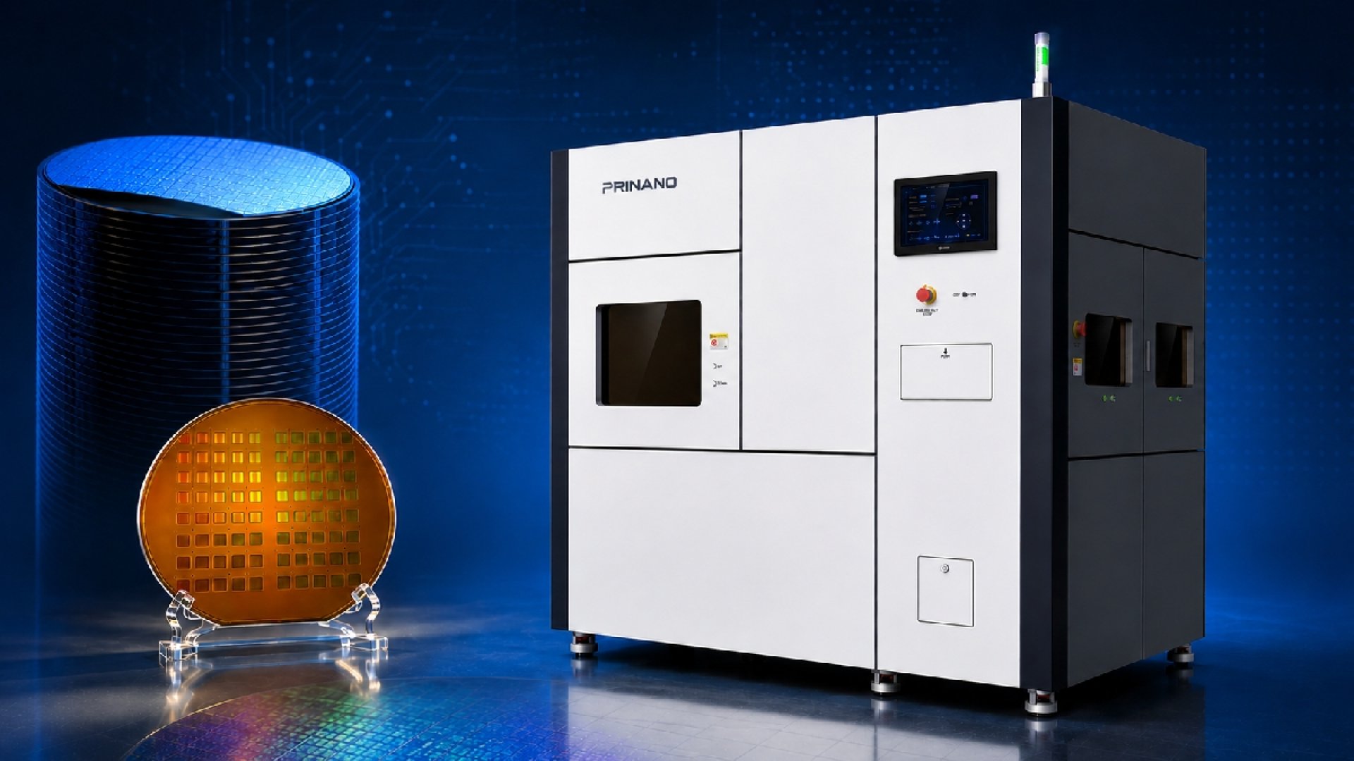
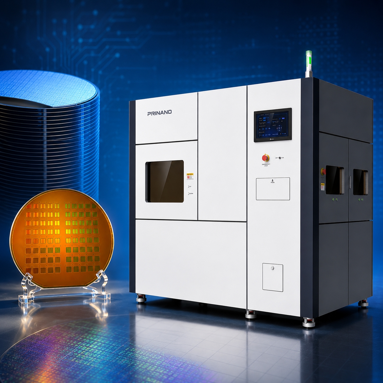
Against this backdrop, on June 5, 2026, Prinano Technology officially delivered its PL-AS vacuum pneumatic wafer-level nanoimprint lithography machine to Shenzhen Lice Technology. At the same time, the two companies announced that they had successfully completed volume-production validation of 8-inch photonic chip wafers using the platform.
The entire manufacturing process was carried out without relying on conventional Deep Ultraviolet (DUV) lithography, reduc
ing per-chip manufacturing costs to approximately one-tenth of those associated with traditional DUV-based solutions.
As the rapid growth of AI computing continues to drive demand for silicon photonic chips, optical communication modules, and optical interconnect devices, Prinano's achievement in full-wafer production not only breaks the long-standing overseas dominance in nanoimprint equipment, but also offers the industry a practical DUV alternative that combines cost efficiency, production-level yield, and scalability.
Prinano's Two Leaps: From "R&D Breakthrough" to "Mass Production Replacement"
Since nanoimprint technology entered the semiconductor industry, only a handful of companies worldwide—such as Canon—have been capable of supplying semiconductor-grade production equipment. Due to export restrictions, domestic wafer manufacturers have long faced difficulties accessing such systems.
In August 2025, Prinano became the first company to break the equipment monopoly by delivering China's first semiconductor-grade step-and-repeat nanoimprint lithography system, the PL-SR. Based on an inkjet-assisted step-and-repeat process, the platform was primarily aimed at process development in advanced integrated circuits and silicon-based microdisplay applications.
The newly delivered PL-AS is a semiconductor-grade vacuum pneumatic nanoimprint lithography machine that represents a major step from equipment development toward process replacement. Rather than adopting a step-and-repeat approach, it utilizes a full-surface contact imprinting architecture specifically designed for wafer-scale production. This makes it particularly suitable for replicating large-area micro- and nanostructures used in photonic chips.
The PL-AS is not a laboratory validation platform. It is a production-oriented system capable of being deployed directly on manufacturing lines, enabling nanoimprint technology to move from process development into large-scale manufacturing.
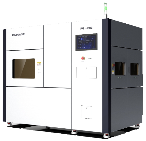
Image source: PRINANO Official Website
From PL-SR to PL-AS, Prinano has achieved more than a simple equipment upgrade. The former addressed whether domestically developed semiconductor-grade nanoimprint equipment could be built; the latter demonstrates whether the technology can achieve stable production, lower costs, and replace selected DUV process steps in photonic chip manufacturing.
Why Can Pneumatic Imprinting Break DUV's Dominance First?
Nanoimprint lithography has long been regarded as one of the strongest challengers to DUV lithography, yet the journey from laboratory research to production deployment has not been straightforward.
Traditional roller-based imprinting offers high throughput, but its line-contact nature often results in uneven residual layer thickness, making it difficult to satisfy the stringent requirements of photonic chip manufacturing. Step-and-repeat imprinting provides excellent precision, but its region-by-region processing inherently limits throughput and makes large-scale manufacturing more challenging.
The vacuum pneumatic architecture adopted by the PL-AS addresses these challenges at a fundamental level.
Its core principle is full-surface contact imprinting. Pneumatic pressure acts like an air cushion, applying uniform force across the entire template. Every nanoscale feature on the wafer experiences consistent pressure, allowing residual layer thickness variation to be controlled below 2 nanometers—a critical threshold in photonic device fabrication.
At the same time, the vacuum environment fundamentally eliminates bubble-related defects and delivers significantly higher filling performance than conventional roller-based processes.
Equally important, the system eliminates the need for the complex and costly optical subsystems required in DUV lithography. This substantially reduces equipment investment and maintenance costs, making large-scale cost reduction possible. According to the company, manufacturing costs can be reduced to approximately one-tenth of conventional DUV-based processes.
In terms of performance, the PL-AS is designed to compete with leading international systems, supporting feature sizes below 10 nanometers, alignment accuracy configurable to within hundreds of nanometers, pressure uniformity errors below 0.5%, and compatibility with both rigid templates and curved substrates.
Multi-Segment Deployment: From "Backup Option" to "First Choice for Mass Production"
The collaboration with Shenzhen Lice Technology is not an isolated case. Prinano's nanoimprint manufacturing solution has already completed customer validation across multiple photonic chip segments.
LiDAR Chips:
Using the PL-AS platform, Shenzhen Lice Technology has achieved scalable production of 18 mm large-aperture optical phased array (OPA) chips, accelerating the commercialization of solid-state LiDAR technology.
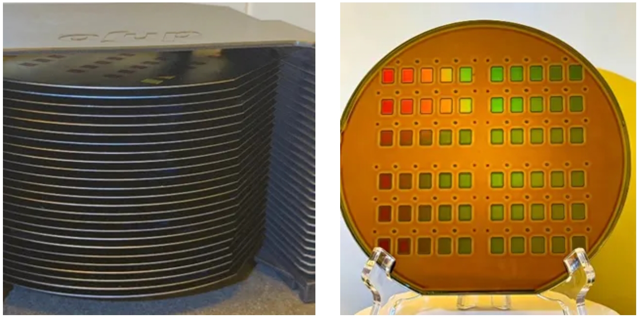
Mass-produced LiDAR chips fabricated using nanoimprint lithography
Optical Communication and Sensing Chips (GaAs/InP):
Through composite-template nanoimprint technology, the challenges associated with fragile GaAs and InP substrates have been addressed, enabling high-fidelity Bragg grating fabrication for leading domestic customers.
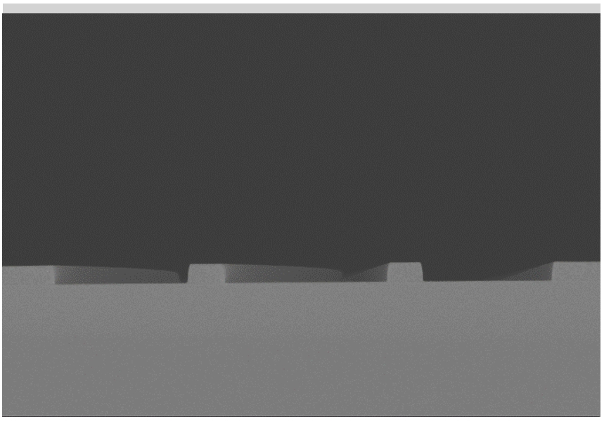
Silicon Photonic Chips:
The company has completed volume-production validation of 8-inch wafer ring-waveguide structures. The process supports one-step fabrication of structures ranging from 150nm to 10μm, while maintaining residual layer thickness below 10 nanometers and sidewall roughness variation below 1 nanometer relative to the imprint template.
Together, these applications point to a broader trend: within the photonic chip sector, nanoimprint lithography is no longer merely a backup option. It is increasingly becoming a preferred manufacturing solution with compelling cost advantages over conventional DUV-based approaches.
3D Perspective: The Deeper Industry Significance of This Delivery
The significance of Prinano's breakthrough in nanoimprint lithography can be understood from three dimensions:
- Technical Dimension, it has proven that domestic nanoimprint can truly replace DUV lithography.
It demonstrates that domestically developed nanoimprint technology can serve as a viable alternative to DUV lithography. This achievement goes beyond laboratory demonstrations, prototype development, or patent workarounds. Through successful volume-production validation on 8-inch wafers, the technology has demonstrated yield and consistency levels suitable for commercial manufacturing.
For an industry long accustomed to viewing lithography primarily through the lens of DUV and EUV, this represents an important shift in perspective.
2. Industrial Dimension, it opens a new low-cost, independently controllable channel for optical chip manufacturing.
It opens a new low-cost and domestically controllable pathway for photonic chip manufacturing.
Photonic devices—including LiDAR chips, optical communication chips, and silicon photonic chips—are highly sensitive to manufacturing costs. The high cost associated with DUV-based production has long constrained large-scale deployment in areas such as autonomous driving and AI optical interconnects.
Reducing manufacturing costs to approximately one-tenth of conventional DUV processes could significantly ease upstream cost pressures and create greater commercial opportunities for downstream innovation.
3. Strategic Dimension, a fully independent closed-loop system of "equipment—materials—processes" has been formed.
It establishes a fully integrated ecosystem spanning equipment, materials, and manufacturing processes.
Prinano simultaneously possesses expertise in pneumatic, roller-based, and step-and-repeat nanoimprint technologies, while also supporting these processes with proprietary dual-layer imprint resist materials.
This means that China possesses not only a single piece of equipment in the nanoimprint sector, but an increasingly complete ecosystem extending from materials and equipment to process integration.
Conclusion: A New Path Defined by China Is Taking Shape
For decades, leadership in semiconductor lithography has been concentrated among equipment suppliers in Europe, the United States, and Japan. China has largely remained in a catch-up position across both DUV and EUV technology pathways.
With the PL-AS, Prinano is demonstrating that, in the strategically important field of photonic chips, Chinese companies are capable of pursuing a different route—one built on process innovation, engineering execution, lower manufacturing costs, and greater technological self-reliance.
As photonic chips continue to play an increasingly important role in AI infrastructure, optical communications, and advanced sensing applications, nanoimprint lithography may be evolving from an alternative technology into a practical manufacturing pathway for next-generation devices.
About Prinano Technology
PRINANO is one of the few teams in China and worldwide that has mastered the core nanoimprint lithography processes, including plate imprinting, pneumatic imprinting, roll-to-roll imprinting, and step-and-repeat imprinting. The company has established a fully integrated industrial ecosystem that deeply combines equipment, materials, and process technologies.
For more information, please visit PRINANO Official Website.
Source : :替代DUV,光芯片赛道迎来国产首台纳米压印光刻机
http://www.semi-insights.com/s/bdt/15/50353.shtml


