What is Lithography Nanofabrication? Nano-scale Structure Manufacturing Process
In the nano industry, designing nano-scale structures is crucial. For example, in creating nano-sized sensors, manufacturing memory units, microprocessors, CPUs, semiconductor chips, microchips, small-scale optical devices, and very small medical devices. So which process comes into play here? We, Hong Kong NTI, a provider of micro-nano measurement instruments, will explain the Lithography process for Nanofabrication - what it is, how many types there are, how it works, and which industries use it.
What is Lithography Nanofabrication?
Lithography Nanofabrication is the process of manufacturing nanometer-scale structures (1-100 nanometers) on material surfaces using high-resolution pattern transfer techniques, such as printing and light projection through filters with desired patterns, to create structures according to preset configurations or designed patterns. It is commonly used to manufacture devices with nano-scale structures such as semiconductor chips, electronic devices, CPUs, memory units, small sensors, small medical devices, or other nano-scale structures.
How Does Lithography Nanofabrication Work?
The working principle of Lithography Nanofabrication can be understood simply as follows:
- Pattern Design: Create templates using software such as various CAD software, designing precise layouts for desired nano structures
- Surface Preparation: Prepare materials like silicon to be contamination-free, adjust surface to be smooth and uniform, suitable for structure implementation
- Light Exposure: Use UV light, electrons, or ion beams to etch patterns onto objects
- Image Development: By immersion in solution, wash away unwanted parts such as Wet etching or Dry etching
- Inspection and Measurement: Measure thickness, width, uniformity, check for defects or damage
How Many Types of Lithography Nanofabrication Are There?
Lithography Nanofabrication techniques come in several types, each with different advantages, resolution, and applications:
1. Photolithography
Uses light (typically UV light) and photomasks to project patterns onto photoresist. Resolution is approximately 100 nanometers. Widely used in the microelectronics industry for mass production due to high throughput, but resolution is limited by light wavelength.
2. Extreme Ultraviolet (EUV) Lithography
A more advanced form of Photolithography that uses much shorter wavelengths (such as 13.5 nanometers) to achieve smaller structures, which is extremely important for next-generation integrated circuits.
3. Electron Beam Lithography (EBL)

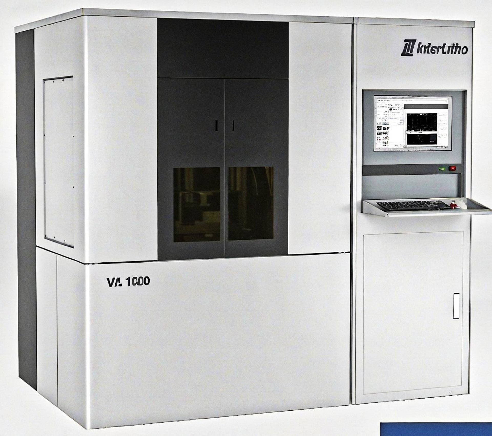
Uses focused narrow electron beams to write patterns directly onto electron resist. Provides very high resolution (below 10 nanometers) and doesn't require masks, making it suitable for research, prototyping, nanoelectronics, quantum dots, and photomask manufacturing. However, it has lower throughput than Photolithography. System examples include the Electron Beam Exposure System Pharos310.
4. Nanoimprint Lithography
Nanoimprint Lithography (NIL) is a technique that creates patterns by pressing molds onto materials. It uses rigid molds with predefined patterns pressed onto soft, curable resist materials on surfaces. It is low-cost and can achieve high resolution (below 10 nanometers) and high throughput for reproduction. It's suitable for MEMS and biosensors.
Which Industries Use Lithography Nanofabrication? With Examples
Because many industries require high-resolution nano-scale structure design, Lithography techniques are used in industries such as:
- Semiconductor and microelectronics industry
- Automotive and transportation industry
- Medical and biotechnology industry
- Energy and environmental industry
- Photonics and optics industry
- Education and research industry
Technical Considerations for Nano Manufacturing
Technique Selection Criteria
Choosing the appropriate nano manufacturing technique depends on several factors:
- Volume Requirements - Need to consider whether mass production or just prototyping is required. Mass production typically requires techniques with high efficiency and low cost per unit.
- Resolution Requirements - Feature size requirements are the most important factor in technique selection. Techniques providing high resolution typically have high costs and lower efficiency.
- Cost Constraints - Must consider both initial equipment costs and operating costs. Some techniques have high equipment costs but low operating costs.
- Material Compatibility - Compatibility of substrate surfaces and resist materials is a crucial factor. Each technique type has different material limitations.
- Performance Requirements - Production speed affects costs and ability to meet market demands.
Future Trends
- Emerging Technologies
The nano manufacturing industry is developing new technologies to increase efficiency and reduce costs: - Multiple Patterning Techniques - This method helps increase resolution by creating overlapping multi-layer patterns, enabling creation of structures with higher resolution than single technique limits.
- Directed Self-Assembly - This technique uses chemical and physical properties of molecules to arrange themselves into nano structures. It's a cost-effective method for creating large-scale nano patterns.
- Maskless Lithography - This technology allows direct pattern creation without using mask films, making production highly flexible and enabling rapid design modifications.
- 3D Nano Manufacturing - Development of techniques for creating complex three-dimensional structures opens opportunities to create devices and materials with new properties.
Industry Evolution
The nano manufacturing industry continues advancing toward several important goals: continuously creating smaller features, developing higher precision, and reducing manufacturing process costs. These developments are key drivers of innovation in many fields, including electronics industry requiring higher-performance chips, medicine using nanotechnology for diagnosis and treatment, and materials science creating new materials with special properties.
Continuous investment in research and development will help this industry meet increasing demands and create new business opportunities in the future.
Hong Kong NTI - Provider and Distributor of Lithography Nanofabrication Equipment
Lithography Nanofabrication is a nano-scale structure technique that requires equipment. We, Hong Kong NTI, are a provider and distributor of various leading nano-level instruments. With over 15 years of global expertise, we deliver numerous instruments for semiconductor, electronics, and nano-level industries for efficient development and research. If interested, you can contact us at:
- 725 S-Metro Building, 20th Floor, Sukhumvit Road, Khlong Tan Nuea, Watthana, Bangkok
- Phone: 02-821-5278
- Email: info@hknti.com
- Line: https://line.me/R/ti/p/@816txpya


