Maskless Future? Hong Kong NTI’s Domestic Direct-Write E-Beam System Enters the Nanofabrication Arena
Semiconductor Industry Observer · August 13, 2026
In advanced micro- and nanofabrication, mention high-resolution lithography and the industry's first reaction is often complex mask-based exposure platforms. However, as demand grows for rapid prototyping, maskless patterning, and sub-10 nm feature control, Direct-Write Electron Beam Lithography (EBL) is emerging as an indispensable pathway. Particularly in high-precision research and specialized commercial fabrication—such as photonic devices, quantum architectures, and high-frequency semiconductors—direct-write EBL offers unmatched flexibility and nanometer-scale accuracy.
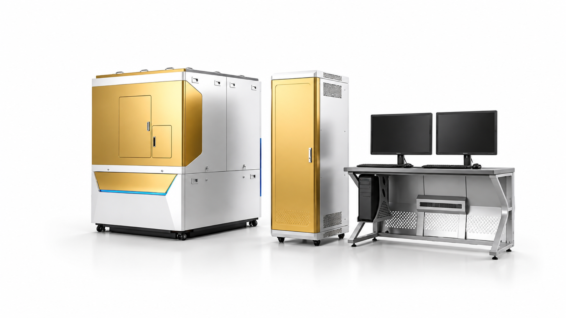
Against this backdrop, Hong Kong NTI Limited has officially launched the EBeam50, a direct-write electron beam lithography system developed entirely in-house from the ground up. Designed as an integrated precision chain, the platform unifies electron-optical design, high-precision stage mechanics, and intelligent pattern control into a single end-to-end manufacturing system.
The entire platform—including the electron-optical column, laser-interferometer stage, and pattern-generation software suite—was built and calibrated completely in-house without reliance on third-party core integration.
As rapid advancements in quantum computing, integrated photonics, and next-generation semiconductors continue to push feature sizes below the 10 nm threshold, NTI's EBeam50 offers the nanofabrication industry a precise, highly stable, and versatile direct-write platform that bridges fundamental R&D with scalable device prototyping.
Three Core Subsystems: From Hardware Breakthrough to Precision Integration
In high-resolution electron beam lithography, the final pattern profile is the combined result of electron optics, mechanical motion, and algorithmic control. Any instability in a single link leaves immediate, visible degradation under an electron microscope. Rather than treating subsystems independently, the EBeam50 treats all three core elements as a single precision chain:
1.The Electron-Optical Column
Powered by a Schottky field-emission electron source, the system provides continuously selectable beam currents from 20 pA to 40 nA. Octupole electrostatic deflection eliminates magnetic hysteresis, while a 50 MHz scan rate delivers a broad process window that balances ultra-fine probe resolution with exposure throughput.
2.The High-Precision Stage
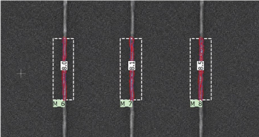
Real-time laser-interferometer positioning is paired with closed-loop motion correction. Standard stage travel is 100 mm, with optional 150 mm and 200 mm configurations available. An automated sample loading mechanism allows fast wafer exchange without breaking main-chamber vacuum, significantly reducing thermal stabilization delays.
3.Pattern Generation and Software Control
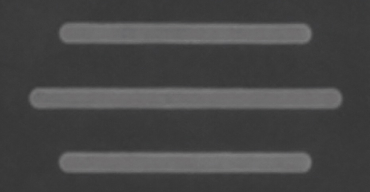
Path planning, proximity-effect dose correction (PEC), autofocus, astigmatism correction, and height tracking are seamlessly unified in one software suite. Complete process parameters can be stored and executed as reusable, transferable recipes.
Why Software-Level Correction Breaks Physical Boundaries First
While hardware stability establishes the system's baseline, software-level control over physical electron-beam interactions provides EBeam50's most distinct practical advantage:
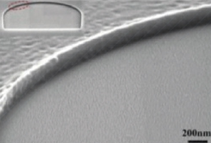
- Contour-Following Path Planning: Conventional raster scanning often introduces edge roughness due to discrete step exposure. EBeam50 supports contour-following exposure, creating smooth, continuous dose accumulation along pattern boundaries—a difference readily visible at the 200 nm scale.
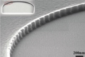
- Proximity-Effect Dose Correction (PEC): Electron backscattering in dense arrays frequently causes resist collapse or overexposure. The EBeam50 dynamically redistributes exposure dosage based on localized pattern density, maintaining uniform energy distribution across dense gratings and isolated lines alike.
Multi-Segment Deployment: From Academic R&D to Industrial Prototyping
The EBeam50 platform has already demonstrated robust performance across a broad range of nanofabrication applications:
- Photonic Devices & Waveguides: Achieves smooth sidewalls and precise cross-sectional profiles in optical waveguides and chirped gratings.
- Quantum & X-Ray Optics: Provides sub-10 nm feature writing necessary for high-fidelity quantum dot layout and binary optical elements.
- Mask & Template Fabrication: Delivers high overlay accuracy (±20nm) across adjacent write fields for large-area template manufacturing.
Strategic Significance: End-to-End Delivery and Ecosystem Support
Hong Kong NTI Limited pairs the EBeam50 platform with a full four-stage delivery support ecosystem:
- Site and Environmental Assessment: Comprehensive survey of vibration, EMI, thermal control, and grounding.
- Installation, Calibration & Acceptance: Rigorous item-by-item verification against contractual metrics.
- First-Article Process Tuning: On-site exposure tuning using the customer's specific resist and substrate system.
- Training & Ongoing Support: Tiered user training, localized spare parts inventory, and integrated remote diagnostics.
Conclusion: A New Standard for Direct-Write Nanofabrication
By unifying electron optics, precision stage control, and software algorithms into a single closed loop, the EBeam50 establishes a highly reliable direct-write EBL solution. With linewidth capabilities reaching below 10 nm and stitching accuracy within ±20nm the platform provides research institutes and semiconductor manufacturers with an agile, high-precision tool to drive next-generation nanostructure development.