
VR - Nanofabrication Processing Coureses
VR - Nanofabrication Processing Coureses
Semiconductor Talent Training Plan Progressive Training System, Goal Programming
Customized courses
Government open courses
Joint development courses with educational institutions (universities, vocational colleges) and practice bases
Pre-employment corporate training: Theory + Practical Training To hit specific customer needs, such as 4 years, 2 years, or short-term.

Fields of Application

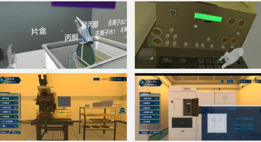
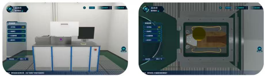
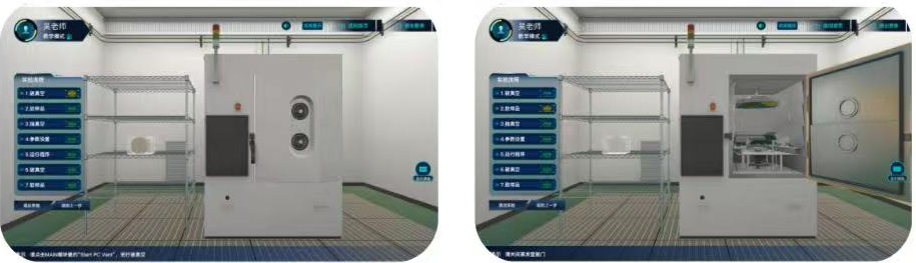
Wafer Cleaning

Photolithography

Contact Exposure Training

Stepper Lithography Training

Magnetron Sputtering Training

VR - Nanofabrication Processing Courses Assistant:
The key findings were:
Immersive and interactive VR system
Wafer Cleaning: Ensures wafer surface cleanliness before entering fabrication steps.
Photolithography: Transfers circuit patterns onto wafer surfaces using mask-based light exposure.
Contact Exposure Training: Develops understanding of contact aligner operation and exposure principles.
Stepper Lithography Training: Differentiates contact and projection exposure techniques and trains on stepper systems.
Magnetron Sputtering Training: Covers thin film deposition techniques using magnetron sputtering.
️
Guaranteed Learning Outcomes
Upon Course Completion:
- Deep understanding of nanofabrication processes
- Industry-ready practical skills
- Reduced onboarding time in real cleanroom environments
- Confidence in precision manufacturing operations
- Comprehensive knowledge of safety protocols
Revolutionary Advantages of VR Training System
Maximum Cost Efficiency
Industry Testimonials
"Our VR training system reduced new employee onboarding time by 70% while improving safety scores by 95%."
"Students now enter our cleanroom with confidence and practical knowledge that would take months to acquire through traditional methods."
The future of nanofabrication education is here!
Start Your VR Journey Today
Immediate access to cutting-edge training
Industry-leading curriculum
Proven learning outcomes
Unmatched cost efficiency
Contact us now to revolutionize your nanofabrication training program!
Competitive Advantages Over Traditional Methods
Speed & Efficiency
Traditional: Weeks of preparation, limited practice time
VR: Instant access, unlimited repetition, accelerated learning curve
Accessibility
Traditional: Geographic limitations, expensive facility access
VR: Global accessibility, 24/7 availability, democratized education
Customization
Traditional: Fixed curriculum, one-size-fits-all approach
VR: Personalized learning paths, adaptive difficulty levels
Performance Tracking
Traditional: Limited assessment capabilities
VR: Real-time analytics, detailed progress reports, skill verification
Revolutionary Advantages of VR Training System
Maximum Cost Efficiency
Traditional Cleanroom: Extremely high construction and maintenance costs (millions of dollars)
VR System: One-time investment, unlimited usage, zero operational costs
Ultimate Safety
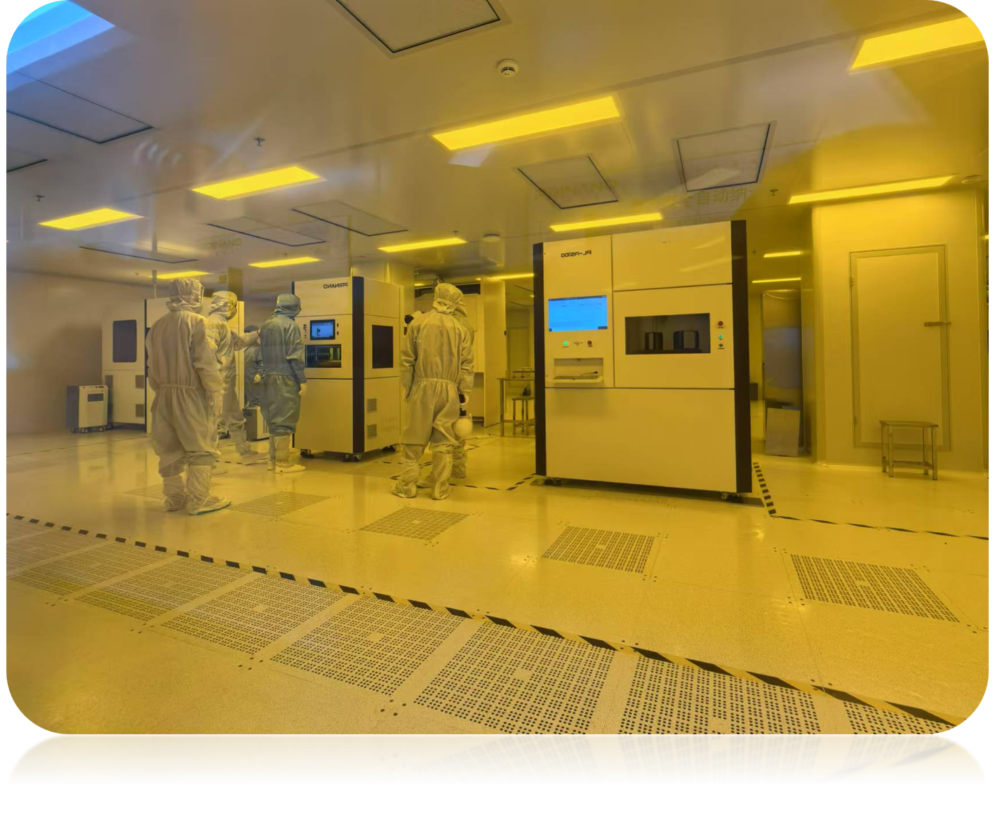
Traditional Cleanroom: High risk from hazardous chemicals, expensive equipment damage, potential accidents
VR System: Risk-free training environment, learn from mistakes without consequences
Superior Learning Effectiveness
Traditional Cleanroom: Limited student capacity, restricted operating hours, limited practice opportunities
VR System: Learn anytime, anywhere, unlimited practice sessions, repeat difficult sections
Lithography instrument
text
Brand:
Samples can be accepted:
Introduction:
Features
Applications

WinSPM EDU
Scanning Probe Coureses
( Microscope Educational System )
WinSPM EDU
Scanning Probe Coureses
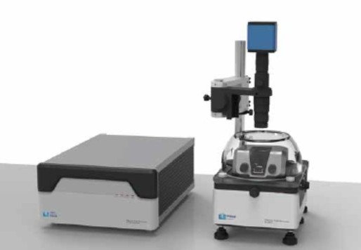
WinSPM EDU: Revolutionary Nanoscience Education Platform
Product Introduction
The WinSPM EDU system was awarded the 'First Prize for National Educational Instruments', honoring its innovative design, reliable performance, and proven utility in advanced nanoscience teaching in universities across China. WinSPM EDU is a scanning probe microscope system tailored for nanoscience education, offering multiple imaging modes, probe types, and intelligent software for experiments, course modules, and research training.
This government-recognized platform combines cutting-edge atomic force microscopy (AFM) and scanning tunneling microscopy (STM) capabilities with intelligent educational software, making advanced nanotechnology accessible to students and researchers alike.
Unlike traditional research instruments adapted for teaching, WinSPM EDU was purpose-built from the ground up for educational excellence.
The system eliminates complex operational barriers while maintaining research-grade performance, enabling institutions to deliver world-class nanoscience education without the typical technical overhead.
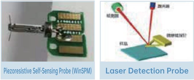
Key Innovation: The first educational SPM system to integrate self-sensing piezoelectric probes, eliminating laser alignment complexity while achieving sub-nanometer resolutionmaking atomic-scale imaging as simple as operating a standard microscope.
Fields of Application for University and Institute Nanotechnology Lab
Semiconductor Process Education and Failure Analysis
Materials Science Research
Optoelectronic Device Characterization
Surface Engineering & Roughness Analysis
Micro/Nano Fabrication Courses
Key Advantages:
- No laser adjustment required, easy and safe operation
- Compatible with self-sensing piezoelectric probes for force curve and nanoindentation analysis
- Compact and integrated design ideal for educational deployment
- Atomic-scale resolution, suitable for advanced education and research training
- Versatile functions cover both research and teaching use cases
- Modular architecture with scalable upgrades and low maintenance cost
Technical Specifications
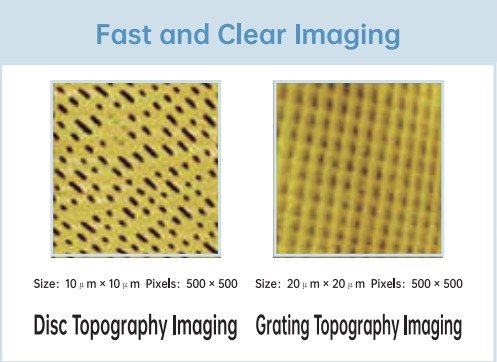
- The multi-environment Atomic Force Microscope (AFM) platform supports various scanning modes, including contact mode, tapping mode, phase imaging, and frequency-modulated topography imaging.
- Compatible with self-sensing piezoelectric probes (Sakaiyama probes), eliminating the need for laser systems and simplifying operation.
- Capable of performing force curve measurements and nanoindentation.
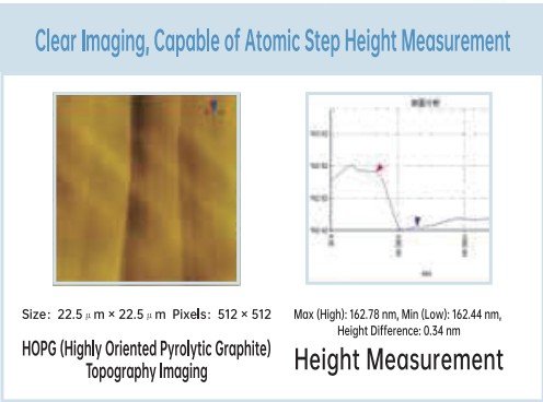
- Minimum scanning range is 20 × 20 × 3 μm³ with a resolution better than 0.1 nm.
- Maximum supported sample size: 20 mm in diameter, up to 5 mm in thickness.
- Supports adjustable scanning range and visualized scan area selection.
- Comes with standard calibration samples and a wide variety of experimental specimens.
- Optional optical modules and educational expansion kits are available.
- Optical modules and video interfaces available
- Educational expansion kits for STEM integration
Proven Applications
Research Capabilities:
- 2D material atomic lattice imaging
- Nanoparticle aggregation analysis
- Biological membrane topography
- Crystalline step height profiling
Teaching Modules
Core Value Propositions
1. Educational Excellence
Purpose-built for teaching: Specifically designed for nanoscience education
Complete curriculum support: Ready-to-use teaching modules and experiments
Student-friendly operation: No complex laser adjustments required
2. Advanced Technology
Atomic-scale resolution: <0.1 nm precision for high-quality research
Multiple imaging modes: Contact, tapping, phase, frequency-modulated topography
Versatile probe compatibility: Self-sensing piezoelectric and laser-based probes
3D analysis capabilities: Force curves, nanoindentation, image reconstruction
3. Practical Advantages
Compact design: Space-efficient for classroom deployment
Safe operation: Simplified controls reduce training time and accidents
Modular architecture: Scalable upgrades with low maintenance costs
Comprehensive software: Built-in analysis, statistics, and 3D rendering
Educational Package Includes
Ready-to-Teach Modules:
- AFM imaging of various samples
- Force curve measurements and nanoindentation
- Surface topography and nanostructure analysis
- STM imaging demonstrations (optional)
- Data processing and 3D image reconstruction
- Sample classification based on image recognition
Industry Applications:
- Semiconductor process education and failure analysis
- Materials science research
- Optoelectronic device characterization
- Surface engineering and roughness analysis
- Micro/nano fabrication course support
Feel free to contact us for detailed technical documents, configuration plans, or to schedule a remote demo and case sharing.

Fields of Application & Services
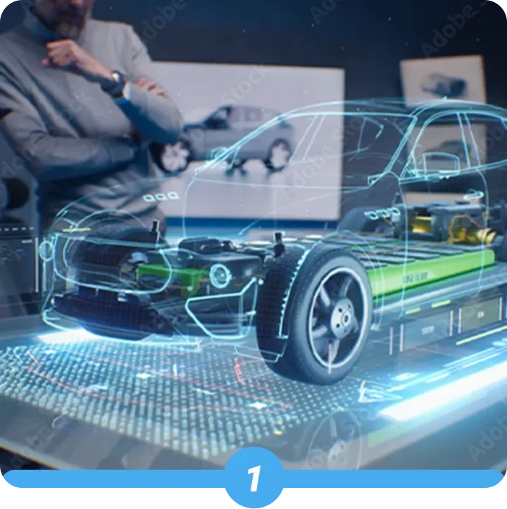
Automobile
Enhancing vehicle performance and safety through advanced material assessment.

Nanoscience
Enabling researchers to examine surfaces at the nanoscale, contributing to innovations in materials and devices.
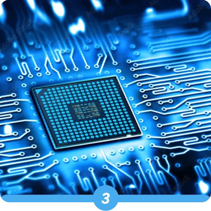
Semiconductor
Providing the precision required for semiconductor manufacturing, from wafer inspection to micro-level surface analysis.

General Consumables (Accessories)

AFM Accessories

SEM Consumables

TEM Consumables

SERS Chip Substrate

GGB Series

