
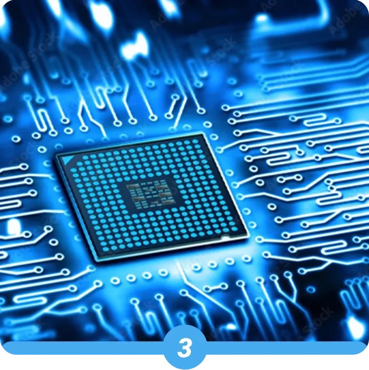
Nanofabrication Coureses
From a blank silicon wafer to functional nano-deviceslearn how precision manufacturing makes modern technology possible.

VR - Nanofabrication Processing Coureses
VR Nanofabrication
Processing Courses
Immersive Virtual Training for Semiconductor and Nanotechnology Manufacturing
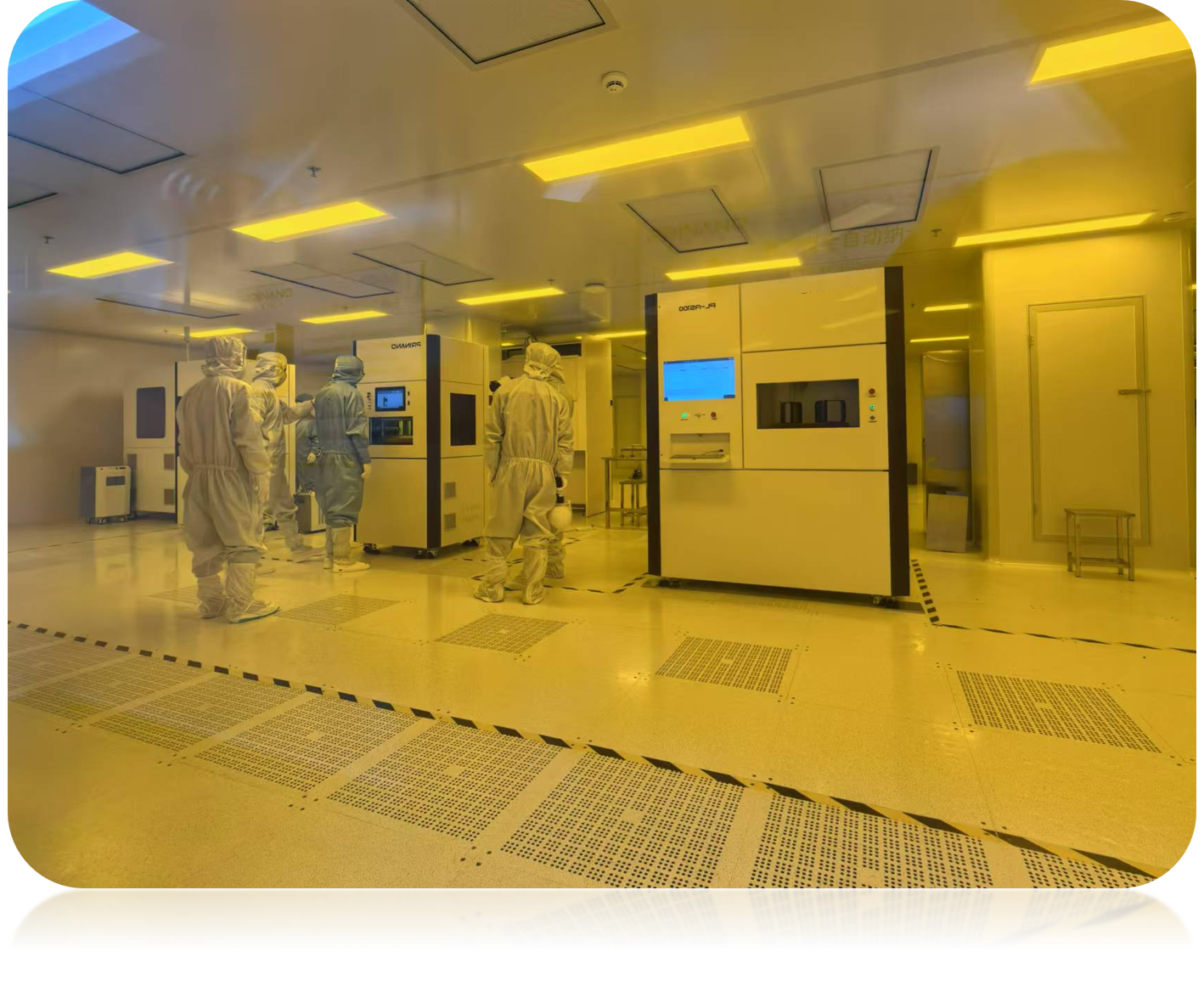
Experience real-world nanofabrication processes through advanced Virtual Reality simulations. Learn cleanroom workflows, fabrication techniques, and industry-standard practicessafely, efficiently, and cost-effectively.
Customized courses
Government open courses
Joint development courses with educational institutions (universities, vocational colleges) and practice bases
Pre-employment corporate training: Theory + Practical Training To hit specific customer needs, such as 4 years, 2 years, or short-term.

Fields of Application

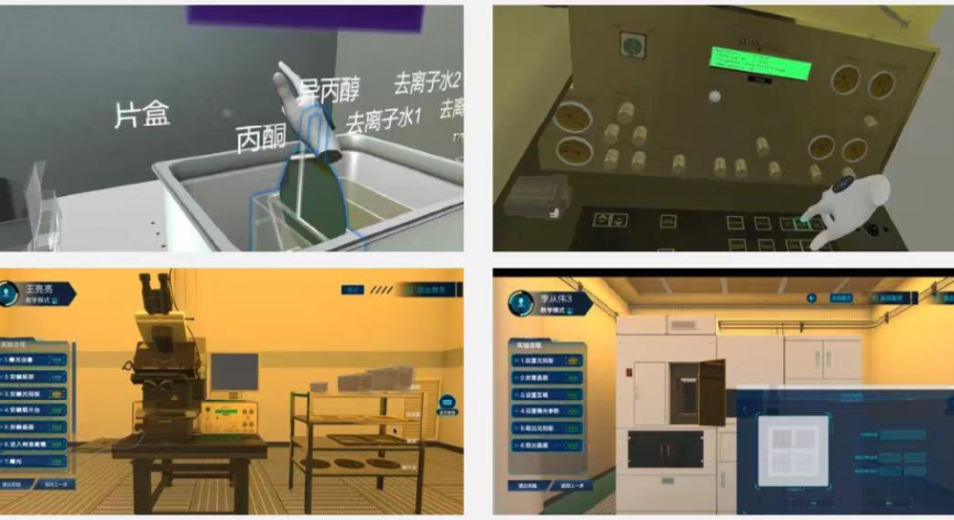
Wafer Cleaning

Photolithography

Contact Exposure Training

Stepper Lithography Training

Magnetron Sputtering Training

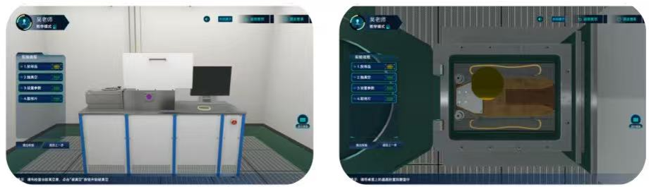
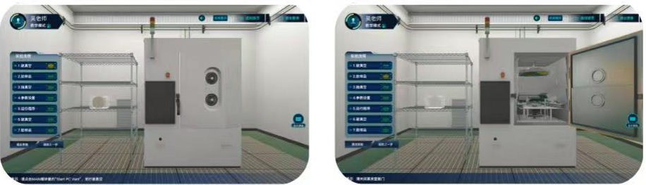
VR - Nanofabrication Processing Courses Assistant:
The key findings were:
Immersive and interactive VR system
Wafer Cleaning: Ensures wafer surface cleanliness before entering fabrication steps.
Photolithography: Transfers circuit patterns onto wafer surfaces using mask-based light exposure.
Contact Exposure Training: Develops understanding of contact aligner operation and exposure principles.
Stepper Lithography Training: Differentiates contact and projection exposure techniques and trains on stepper systems.
Magnetron Sputtering Training: Covers thin film deposition techniques using magnetron sputtering.
️
Guaranteed Learning Outcomes
Upon Course Completion:
- Deep understanding of nanofabrication processes
- Industry-ready practical skills
- Reduced onboarding time in real cleanroom environments
- Confidence in precision manufacturing operations
- Comprehensive knowledge of safety protocols
Revolutionary Advantages of VR Training System
Maximum Cost Efficiency
Industry Testimonials
"Our VR training system reduced new employee onboarding time by 70% while improving safety scores by 95%."
"Students now enter our cleanroom with confidence and practical knowledge that would take months to acquire through traditional methods."
The future of nanofabrication education is here!
Start Your VR Journey Today
Immediate access to cutting-edge training
Industry-leading curriculum
Proven learning outcomes
Unmatched cost efficiency
Contact us now to revolutionize your nanofabrication training program!
Competitive Advantages Over Traditional Methods
Speed & Efficiency
Traditional: Weeks of preparation, limited practice time
VR: Instant access, unlimited repetition, accelerated learning curve
Accessibility
Traditional: Geographic limitations, expensive facility access
VR: Global accessibility, 24/7 availability, democratized education
Customization
Traditional: Fixed curriculum, one-size-fits-all approach
VR: Personalized learning paths, adaptive difficulty levels
Performance Tracking
Traditional: Limited assessment capabilities
VR: Real-time analytics, detailed progress reports, skill verification
Revolutionary Advantages of VR Training System
Maximum Cost Efficiency
Traditional Cleanroom: Extremely high construction and maintenance costs (millions of dollars)
VR System: One-time investment, unlimited usage, zero operational costs
Ultimate Safety
Traditional Cleanroom: High risk from hazardous chemicals, expensive equipment damage, potential accidents
VR System: Risk-free training environment, learn from mistakes without consequences
Superior Learning Effectiveness
Traditional Cleanroom: Limited student capacity, restricted operating hours, limited practice opportunities
VR System: Learn anytime, anywhere, unlimited practice sessions, repeat difficult sections
Get to know more about the Courses & Instrument

Metrology Measurement Courses
Metrology Measurement Courses
Precision Measurement & Characterization for Advanced Manufacturing
Develop essential skills in dimensional measurement, surface analysis, and nano-scale characterization to ensure quality, accuracy, and reliability in manufacturing and research.
Fields of Application for University and Institute Nanotechnology Lab
Dimensional & Thickness Measurement
Surface & Roughness Analysis
Thin Film & Material Characterization
Surface Engineering & Roughness Analysis
Micro/Nano Fabrication Courses
Typical Instruments Covered
Training content aligns with commonly used metrology systems, such as
- Stylus Profilers for surface and step-height measurement
- Atomic Force Microscopes (AFM) for nanoscale characterization
- Optical Metrology Systems for non-contact measurement
- Advanced nano-measurement platforms
What You Will Learn
Participants will be trained in core metrology and characterization techniques, including:
Dimensional Measurement
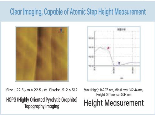
Measure critical dimensions, step height, and film thickness with high accuracy and repeatability.
Surface & Roughness Measurement
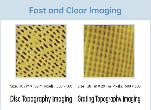
Analyze surface topography, roughness, and texture to evaluate material and device performance.
Thin Film & Material Characterization
Understand measurement techniques for thin film thickness, uniformity, and material properties.
Imaging & Defect Inspection
Learn inspection and imaging methods to identify defects and structural deviations at micro- and nano-scales.
Data Analysis & Interpretation
Develop skills in analyzing measurement results, evaluating uncertainty, and generating professional reports.
Learning Outcomes
Upon completion, participants will be able to
- Select appropriate measurement techniques for specific applications
- Operate precision metrology instruments effectively
- Interpret data accurately for QC and R&D purposes
- Improve process control and manufacturing yield
- Support advanced research and product development
Why Metrology Matters
Precision metrology is essential for
- Ensuring compliance with design specifications
- Reducing defects and improving yield
- Supporting continuous process improvement
- Enabling reliable innovation in nanotechnology and semiconductor industries

Fields of Application & Services
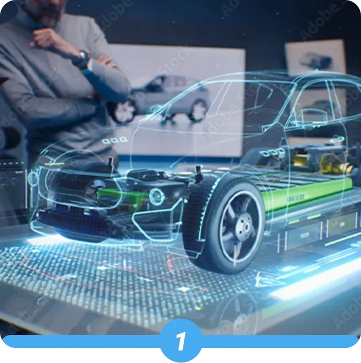
Automobile
Enhancing vehicle performance and safety through advanced material assessment.
Nanoscience
Enabling researchers to examine surfaces at the nanoscale, contributing to innovations in materials and devices.
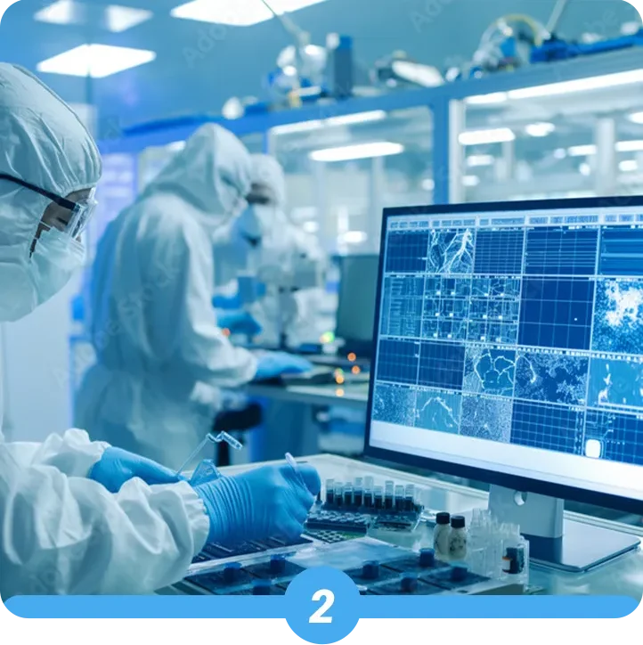
Semiconductor
Providing the precision required for semiconductor manufacturing, from wafer inspection to micro-level surface analysis.